Robert Aalund
Business Development Manager, SPS Technology
Thermal Technology LLC
Santa Rosa, California
Now and again a technology finds a niche and quickly becomes the standard process within that industry. Then people look back and wonder how they ever got along without that new standard. Spark Plasma Sintering or SPS has this kind of potential in many industries. With the ability to produce near-net and net shapes directly from powder at less than 10% the expense of conventional processing, certainly SPS should be taken seriously. This report details one example of how SPS can be applied commercially today, with enormous economic benefits.
SPS has been around since the early 90s. Indeed, SPS-like technology has been around for substantially longer. Though there have been attempts to apply SPS on a few commercial applications, by far the majority of interest has been in R&D and academia.
There are several very basic reasons for SPS technology’s slow migration to commercial use. First and foremost, the few attempts at commercial applications have been collaborations between SPS manufacturers and end users, with many sensitive details divulged between the two, and non-disclosure agreements limiting future discussions. This lack of discourse and the general “black box” view of SPS has resulted in a very slow migration from academic and R&D to commercial use.
Second, SPS requires a significant up-front investment in time and expense. The operational variables include, but are not limited to, material properties, die design and material, heat ramp rates, hold temperatures and times, force strategies, vacuum and atmospheric conditions, power settings and cooling conditions. Commonly, test samples require sophisticated analysis. This development is necessary to draw the most benefits from SPS technology. These variables need to be examined thoroughly before a high throughput strategy can be built around an application. There are many examples of promising high throughput SPS applications that have been dropped as the end user becomes overwhelmed or impatient during the sample development stage.
Third, an important SPS market is only now emerging. Though there are many benefits to SPS processing, one of the most important is its ability to process very fine particulate materials with minimal grain growth and minimal negative effect on micro structure. Due in part to SPS technology, many advanced super fine particle materials are only now becoming available on a commercial level.
A Brief Review of the SPS Process and Some of its Benefits
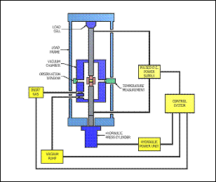
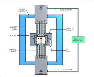
Spark plasma sintering (SPS) is a high-speed powder consolidation/sintering technology capable of processing conductive and nonconductive powder materials. SPS utilizes uniaxial force and applies ON-OFF DC pulse current directly through the cold rams, die, and material. (figure 2) The current creates extremely high heat at the contact points between particles. The ON-OFF DC pulse disperses the heat phenomena throughout the specimen, resulting in a rapid and thorough heat distribution, high homogeneity, and in the end, consistent densities – be they high densities or controlled porosity.
SPS’ operational or “monitored” temperatures (200-2400°C) are commonly 200 to 500°C lower than with conventional sintering, classifying SPS as a lower-temperature sintering technology. Material processing (pressure and temperature rise and hold time) is completed in short periods of commonly 2 to 25 minutes. The relatively low average temperatures combined with fast processing times ensure tight control over grain growth and microstructure.
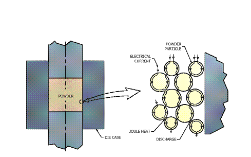
Theories on the spark plasma sintering process vary. Originally, the most commonly accepted theory was the micro-spark/plasma concept. This was based on an electrical spark discharge phenomenon caused by high-energy, low-voltage, pulse DC current momentarily generating spark plasma at high temperatures (many thousands of °C) in fine areas between the particles. (figure 3) This is how the name Spark Plasma Sintering was established. This theory is still accepted by some researchers. They suggest that even in a vacuum atmosphere, when heat and pressure are applied to the material, out-gassing takes place on the surface of the particles, and this provides an adequate atmosphere to establish very fine plasma. In this case, the initial heat is resistive – generated within the die and/or material. Others believe the entire process is simply local particle to particle resistive heating.
In the case of non-conductive material, the process starts out as resistive heat generated within the die. But as the die temperature increases, the current resistance of the material drops, and at some point, current begins to flow through the material.
Regardless of theory, many researchers are very intrigued with SPS technology. There have been volumes of papers written indicating unique particulate bonding properties, minimal grain growth, benefits regarding micro structure, high density and controlled porosity, and homogeneity in mixed and layered materials. As a result, interest in SPS technology within the academic and research community continues to build worldwide.
Commercial Processing With SPS Technology
There are differing approaches to volume processing with SPS technology. The simplest being batch processing. This is where two or more parts or “samples” are made during one cycle. Commonly, in the case of flat shapes, samples can be stacked within the die, using die spacers. Parts can also be oriented in a circular fashion around a circular die such as the hour markings on a clock. And it’s certainly possible to combine both. The key is that both force and electrical density need to be applied evenly across all the samples within the die. This is where tooling design becomes critical.
Aside from batch processing, there have only been a few attempts, worldwide, at applying genuine high throughput and automation to SPS technology. Unfortunately as mentioned above, gathering detailed information on them is nearly impossible.
The Thermal Technology Approach
The key to advancing SPS technology within the commercial industry lies in the development of an efficient, high quality, reliable high throughput system. The ideal system should have a minimal footprint and only one SPS processing section or press chamber. It must produce high volume output and include a strategy for protecting the die during disassembly. Lastly, the price needs to be reasonable per the potential part volume. These conditions must be met in order to successfully usher SPS technology into true, economically sound, commercial use.
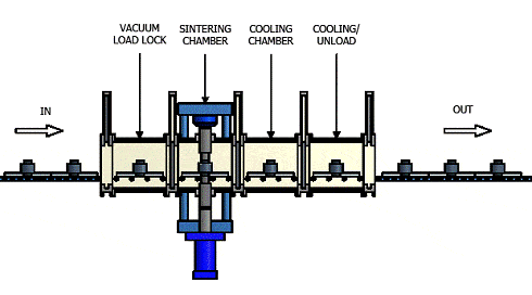
Thermal Technology’s patented High Throughput (HT) SPS design addresses all the above requirements. The process operates as follows:
-Section one – two stage glove box
- First stage – load material into the die (atmosphere controlled fill hopper)Second stage – die assembly
- Second stage – die assembly
Section two – press chamber (SPS operation and die striping)First stage – SPS heat/force cycle
- First stage – SPS heat/force cycle
- Second stage – the die is “hot-stripped”Section three – seven stage cooling carousel
Section three – seven stage cooling carousel
Section four – load lock chamber for die-set removal
Notes:
- The die-set is automatically moved throughout the system on three separate reciprocating carriages.
- The press chamber isolation valves are water cooled.
- Hot-stripping the die immediately after processing is critical. If the die-set is allowed to cool while assembled, there can be substantial scoring damage on the die during disassembly because the material and die cool at different rates. Hot stripping the die prevents this damage.
- The cooling chamber stages can be increased or decreased, depending on cooling needs.
The entire system is controlled via a single control unit with each individual step programmed using macro variables. Meaning the process movements are triggered by other processes, not just timed. Also, the entire system is controlled and protected by a complex set of macro variables, and interconnect and thermal switches.
About SPS Tooling
Tooling requirements and processing issues must be weighed carefully before settling on a final design. Tooling strategies are commonly pre-tested and may include several layers of materials, including semiconductor, non-conductive, and strength materials.
Generally, when processing high temperature materials, above 1200°C, graphite is the norm. SPS graphite tooling is generally made of fine grain, high strength, high density, very high purity material. It has a very high melting temperature, is a good semiconductor, it is relatively inexpensive, and is easy to machine. Graphite also produces a reducing atmosphere within the tooling during processing. This can be very valuable when processing materials that are easily oxidized.
The negative aspects of graphite include possible carbon contamination, high wear, and low compressive and flexural strength. This means net shaping is not likely unless the final parts do not require tight tolerances. It also means tools need to be routinely replaced due to high wear and breakage.
Other tooling materials include tool steels, tungsten carbide, and ceramics doped with conductive materials. All these choices work well with high volume and net shaping applications, but have limited temperature capacities. Generally, max processing temperatures for a given tooling material falls in the range of 60% of the melting temperature of the tooling, which is the lowest temperature material in the mix if it’s a composite.
Negative aspects of high strength materials include high cost and chemical incompatibility with required atmospheres and processing materials.
As mentioned above, it’s not uncommon to insert a graphite sleeve in a high strength die material. This combines all the benefits of graphite with the strength of steels or ceramics, plus the insert is relatively inexpensive to replace.
Net, Near-Net, and Binder-Less Part of Processing
Binder-less processing and net and near-net processing are major benefits of the SPS process. Because SPS technology does not require binders to bond powders, the pre-press operation or “green” stage is unnecessary. With high strength tooling, net and near-net shaping is possible with limitations. One is size. The largest parts that have been produced using SPS are in the range of 450mm diameter x 7mm thick.
Some shapes are more easily processed with SPS technology, others may require multiple procedures. The primary issues are force and electrical density. If force and electrical density can be maintained evenly throughout 100% of the part, it qualifies as a candidate for SPS processing. Others may not lend themselves to a single SPS process, but bonding is always an option. It is possible to bond finished shapes using SPS. In fact, it is possible to bond like and dissimilar materials with SPS. The contact points where shapes have been bonded can have very high strength, in many cases rivaling the strength of the base materials. This effectively minimizes traditional secondary machining.
The True Cost of High Throughput SPS Processing
Though there are many potential commercial applications for SPS technology, we’ll discuss only one example in detail. This study does not include peripheral expenses such as the cost of material, material preparation, labor, or post processing expenses. This is an examination of just SPS operation and consumables.
The example product is a 200mm diameter x 10mm thick sputtering target with an approximate processing temperature of 1800°C. It is assumed full density is required (above 98% relative density). Processing cycle times (ramp up and hold) are in the range of 14 minutes for one part and 17 minutes when two parts are stacked in the die. This example details the latter (two plates per run). Note: There is minimal out-gassing during processing, meaning there is no need to suspend processing so vacuum can catch up.
In detailing total processing cycle times, we need to re-examine the process steps previously listed. Assuming this is an ongoing process, it’s safe to say the operator will load the empty die-set into the glove box while the SPS is processing another die-set. While in the glove box, the die is filled, weighed, vibrated, assemble, and lightly pre-pressed. At this time the operator activates the “ready” switch, notifying the control that the die-set is ready to be moved into the press chamber.
In the press chamber, as soon as the previous sample’s hold time is complete and the die is hot stripped, the die-set is then moved into the seven stage cooling chamber. Because the cooling chamber and the press chamber use the same atmosphere, very little vacuum is lost. Then the next die-set is loaded into the press chamber. If the following die-set is not in location and the operator has not hit the “ready” switch, the system simply waits until the switch is activated.
After seven cooling cycles the die-sets are moved into the exit load-lock chamber and the atmosphere is neutralized. The operator is then notified that the load-lock chamber is ready for unloading.
This is the time cycle breakdown:
- SPS processing 17.00 min.
- Cooling isolation valve opens .25 min.
- Cooling carriage moves into chamber .75 min.
- Die-set and part transfer to carriage .50 min.
- Carriage moves out (while loading isolation valve opens) .75 min.
- Load carriage moves into press chamber .75 min.
- Close load isolation valve .25 min
- Vacuum pump down (may not be needed) 3.00 min
_________________________________________________________________________________________________________________________________
Total cycle time: 23.25 min
Rounded to a 24 minute cycle time, this would equate to 60 SPS cycles or 120 sputtering targets in 24 hours. With six day processing, that’s 720 plates/week, or 2880 in a month.
Any high throughput system will require regular cleaning and lubrication, plus ongoing minor adjustments. It is recommended that users of such a system plan for one day of down time for each six full days of operation.
Required utilities include power, water, and compressed air. Max power consumption is estimated at 780kVA. Maximum power is active during roughly 71% of the cycle (17 of 24 minutes) otherwise, the system is running on approximately 20kVA. In a given week, which would include 20kVA for power usage during maintenance, total power consumption would be in the range of 81,016kWh. At today’s energy costs (the 2008 US national average was $.11 per kWh), that would average approximately $8,900/week.
- 71% of 24 hours = 17.03 hours at max power
- 29% of 24 hours = 6.96 hours general operation
- 17.03 hours x 6 days = 102.18 hours/week at max power
- 6.96 hours x 6 days = 41.76 hours/week general operation – Add 24 hours/week general operation during maintenance (65.76 hours/week general operation)
- Total kilowatt hours per week = 81,016 ((780 x 102.18) + (20 x 65.76) = 81,016) – Note: kVA converts almost exactly into kWh
- 81,016 x $.11/hour = $8,911.76/week
The ongoing expense of operating a cooling tower and utilizing compressed air is approximately $100 each/week.
For this example, 10 complete graphite die-sets are required at approximately $10,000 per set – included in system price. Regarding ongoing die-set expenses, two strategies are utilized to minimize ongoing tooling expenses: hot stripping the die and using replaceable die inserts and punch surfaces. These replacement inserts are estimated to cost around $1,500.00/set. We estimate insert replacement every 50 runs. At 60 cycles/day using 10 die-sets, each die-set is used 6 times daily. With a six day a week processing cycle, that’s a replacement every 1.39 weeks. In breaking the cost down to a weekly estimate, that’s $1079.12 per week per set (1500/1.39), or $10,791 for all ten sets.
Converting expenses in monthly terms:
- Power $35,648
- Water $400
- Air $400
- Tooling $43,164
Total monthly operational expenses: $79,612
Regarding equipment expense, a budgetary quote for the system detailed in this report, including initial tooling, is $2.8M. For this example, we’ll depreciate the total initial expense over 8 years. This puts a total monthly purchase burden of $29,167 on this system ($2.8M /8 = $350K per year /12 = 29,166.66). So the total monthly expenses associated with this system and this application is: $108,779.
Note: As mentioned earlier, we are only detailing the SPS purchase cost, utilities, and tooling. All other expense estimates would vary from facility to facility.
Hot isostatic pressing (HIP) and hot pressing (HP) are the standard conventional technologies for consolidating powder sputtering targets. Commonly with targets this size, manufacturing, including consolidation, secondary machining, labor, and general business expenses run in the range of $1000 to $1200 per target. And generally, the consolidation process and equipment (including equipment purchase and depreciation) would cover approximately 40% of these values. That’s $400.00 to $480.00 per target in consolidation expenses, not including labor. Comparatively, with the Thermal Technology High Throughput SPS system, the cost of consolidation is $37.77 per target ($108,779/2880 plates).
SPS processing of both larger and smaller sputtering targets is equally interesting. In the case of 350mm targets, the general approach is the same. The processing time per press increases to 25 minutes with a 32 minute cycle. That’s 90 targets per day, with similar general expenses and an increase in power consumption. After calculation, the cost per target is $52.
In the case of 50mm targets, the throughput per press is 36 targets (3 targets stacked in a clock face die design). With similar processing expenses and cycle times, the throughput is 2160 targets per day. After calculation, the cost per target is $2.09.
As a reminder, if processing lower temperature materials, high strength tooling can be used. This opens the door to net shaping (minimal or no secondary machining), increasing profitability even further.
As mentioned above, the materials used in these examples produce minimal out gassing during processing, and there was no need to suspend processing for vacuum. Many materials do out-gas heavily during processing, especially in volume processing. Let’s consider the 200mm plate example above with a 57 minute cycle. (Approximately 20 minutes at full power (780kVA), 30 minutes of 20% power (158kVA), and 7 minutes at 20kVA.) In this scenario the throughput drops to 50 plates per day, but the power consumption and the tooling expenses also drop. When calculated, the cost per plate only rises to $59.11. Still a huge savings compared to conventional processing!
So Why Isn’t Everyone Using SPS?
SPS high throughput technology is an innovation whose time has come. Previous impediments to growth have been removed with the development of a truly comprehensive, commercial high throughput system. Thermal Technology LLC has a great deal of confidence in the economic soundness and viability of this important new technology. We routinely see serious interest from a broad spectrum of industries, and foresee tremendous growth in high throughput SPS technology.

